ALMA Project Book, Chapter 9.
IF Processing and Signal Transmission
R. Sramek, W. Brundage,
J. Jackson, A. Baudry
2001-January-30
Revision History:
2000-December-12:
First Completed Version2001-January-30: Revised section 9.2 and 9.3; digitizer interface to the data-transmission system now 250 Mb/s; options for the Fast Demultiplexing Unit discussed. Minor text changes in section 9.1, 9.2.3, 9.3
Summary
The signal processing at the antenna from the IF (intermediate frequency) outputs of the Front-End to the digital inputs of the correlator is described in this chapter; the subsections are:
9.1) the Downconverter
9.2) the Digitizers
9.3) the Fiber Optic Data Transmission System.
The signals from the active front end at each antenna will pass through an IF selector switch within the front end package and then into the IF Downconverter. The Downconverter output signals will then go to Digitizers, then to the Data Transmission System, which will carry the digital signals to the central electronics building, then to the correlator.
9.1 The Downconverter
In each ALMA antenna there will be two Downconverter modules, one for each polarization, and the two inputs to each module will carry upper and lower side-band signals.
A block diagram of the Downconverter is shown in Figure 9.1.1 and the specifications are in Table 9.1.1 The input and output noise power spectral power distribution will be nominally flat over the passband as given in the specifications.
The Downconverter will take the wideband 4 - 12 GHz input signals received from the front end subsystem and produce four output signal channels each with a passband of 2 - 4 GHz suitable for bandpass sampling at by the digitizers, which are clocked at 4 GS/s
In addition to gain, frequency conversion and passband definition, the Downconverter module provides total power measurement of both the wideband input signal channels and the four octave band output channels. Also it provides switching which allows any output channel to tune either the upper (8 - 12 GHz) or lower (4 - 8 GHz) frequency portion of either input channel. The frequency tuning is provided by LO inputs in the 8 - 14 GHz range from four second LO
synthesizers.
Table 9.1.1 Specifications for Downconverter
DOWNCONVERTER MODULE
SPECIFICATIONS for ALMA CONSTRUCTION
Document # ALMA06002NX0002
2000 November 15
W. D. Brundage
Reference: Block Diagram, Document # ALMA06002KX0002
* indicates interfaces
|
Number of modules |
142 (2 x 64 antennas plus 14 spares) |
|
*Inputs from front end |
|
|
Number of inputs per module |
Two: USB, LSB (upper and lower sidebands) |
|
Frequency range, nominal |
4-12 GHz or 4-8 GHz |
|
Power level within any 2 GHz bandwidth when the antenna temperature is 290K |
-40 +/-3 dBm, less loss of coax and connectors between front end outputs and module inputs (3m of phase stabilized Andrew FSJ1P-50A ¼ inch diameter, attenuation = 2.4 dB @ 12GHz) |
|
Variation of power spectral density vs. frequency (flatness) |
<+/-1.5 dB across the nominal frequency range |
|
Headroom when the antenna temperature is 290K (see definition) |
>20 dB |
|
*Inputs from Second LO (LO2) |
|
|
Number of inputs per module |
Four (A, B, C, D), independently tunable |
|
Frequency range |
8.0-14.0 GHz nominal; frequency LO2 > frequency input |
|
Power level |
+13 +/-1 dBm |
|
Power level of spurious frequencies |
<-70 dBc, except <-40 dBc for 2nd harmonic |
|
*Outputs to digitizers |
|
|
Number of outputs per module |
Four (A, B, C, D) |
|
Frequency range |
2 - 4 GHz nominal |
|
Power level |
-TBD +/-TBD dBm plus loss of coax and connectors between output and input to digitizer module |
|
Headroom when the antenna temperature is 290K |
>20 dB |
|
LO2 spurious and leakage at outputs |
<(power level -40 dB) for all combinations of frequencies of LO2-A, -B, -C, -D |
|
Throughput from front end inputs to outputs to digitizers |
|
|
Input S11 reflection magnitude 4 – 12 GHz |
<-20 dB (VSWR < 1.22) to minimize spectral ripples |
|
Input noise figure 4 – 12 GHz |
< 10 dB (2 610K); SPDC < -164 dBm/Hz << SPFE = -133 dBm/Hz |
|
Image rejection |
>20 dB |
|
Filter, 4-12 GHz nominal bandpass for total power detection |
passband <4.0 GHz and >12.0 GHz at -1 dB, max ripple +/-0.5 dB; stopband 3.5 GHz and 12.5 GHz at < -20 dB, 0-3.0 GHz and 13.0-18 GHz at < -40 dB |
|
Filter, bandpass image reject
|
(may be revised after re-analysis of spurious mixer responses) |
|
4-8 GHz nominal |
passband <4.1 GHz and >8.4 GHz at -1 dB, max ripple +/-0.5 dB; stopband 4.0 GHz and 8.6 GHz at < -10dB, 0-3.0 GHz and 10-18 GHz at < -40 dB |
|
8-12 GHz nominal |
passband <7.6 GHz and >12.0 GHz at -1 dB, max ripple +/-0.5 dB; stopband 7.4 GHz and 12.4 GHz at < -10 dB, 0-6.0 GHz and 14-18 GHz at < -40 dB |
|
Filter, outputs A, B, C, D (may be revised after re-analysis of mixer and digitizer spurious responses) |
passband <2.1 GHz and >3.9 GHz at -1 dB, max ripple +/- 0.5 dB; stopband 0-2.0 GHz and 4.0-12 GHz at < -20 dB |
|
Passband amplitude ripple |
<1.0 dB peak-peak |
|
Passband deviation from linear phase |
<40 degree peak-peak |
|
Gain stability |
<0.1 dB peak-peak over 1 minute, <0.5 dB peak-peak over 60 minutes |
|
Phase/delay stability |
<10 degree peak-peak over 1 minute, <40 degree peak-peak over 60 minutes |
|
Headroom1 when the antenna temperature is 290K |
>20 dB |
|
Crosstalk (inverse of isolation) among any input and any unconnected output |
>40 dB rejection |
|
Attenuators in input path 4-12 GHz |
|
|
Steps |
1 +/-0.3 dB |
|
Range |
>30 dB |
|
Phase variation vs. attenuation |
<20 degree peak-peak over attenuation range 0-20 dB |
|
Deviation from linear phase vs. frequency 4-12GHz |
<20 degree peak-peak over attenuation range 0-20 dB |
|
Attenuators in output path 2 - 4 GHz |
|
|
Steps, nominal |
0.25 +/-0.15 dB over attenuation range 0-20 dB |
|
Range, nominal |
>30 dB |
|
Phase variation vs. attenuation |
<10 degree peak-peak over attenuation range 0-20 dB |
|
Deviation from linear phase vs. input frequency 4-12 GHz |
<10 degree peak-peak over attenuation range 0-20 dB |
|
Matching among all downconverters |
|
|
Amplitude vs. frequency |
TBD |
|
Phase vs. frequency |
TBD |
|
Total power detectors (TPD) |
|
|
Input path 4-12 GHz |
|
|
Number |
two, one for each input channel |
|
Response vs. input frequency at any LO2 frequency |
< 2 dB peak-peak. |
|
Output path 2 - 4 GHz |
|
|
Number |
four, one for each output channel A, B, C, D |
|
Response vs. input frequency at any LO2 frequency |
< 1.5 dB peak-peak. |
|
Linearity |
<1 % deviation from square law over range -6 dB to +13 dB relative to antenna temperature = 290 K |
|
Monotonic resolution of digitizer, minimum |
16 bits for 13 dB headroom above antenna temperature = 290 K |
|
*Readout |
2 millisec integrations and dumps to MC-AMBTP card via serial or parallel interface |
|
*Offset calibration |
MC sets the input power to zero by either setting the preceding attenuator to >(20 dB + headroom) or by removing bias to the preceding amplifier |
|
Stability of output relative to inputs from front end |
<50 ppm in 1 second, <500 ppm in 60 seconds |
|
*Interface to MC-AMBTP |
dedicated total power data link to antenna bus master (ABM) |
|
*MC control functions |
|
|
Set levels of input total power detectors |
1 byte for each of two attenuators |
|
Set levels of output of each total power detector and input level of each output digitizer |
1 byte for each of four attenuators |
|
Set to zero all inputs to total power detectors |
1 byte to remove bias to six amplifiers; or set all attenuators to maximum |
|
Set all 3 matrix switches (select image filters for each output) |
1 byte |
|
*MC monitor functions |
|
|
Total power detectors |
3 bytes every 2 milliseconds for each of 6 detectors |
|
Temperatures |
2 bytes every 10 seconds for each of 8 locations |
|
Supply voltages derived within module |
2 bytes every 10 seconds for each of 8 voltages |
|
*External power supply inputs |
+18 +/-0.5VDC @ <2.2A, -18 +/-0.5VDC @ <0.7A, +8 +/-0.3VDC @ <0.6A, +5 +/-0.1VDC @ <0.6A |
|
Internal voltage regulators |
|
|
Output voltages @ amperes |
+15 @ 2.2 (total of >1 regulator), -15 @ 0.6, +5 @ 0.6, -5 @ 0.1 |
|
Output regulation plus noise |
0.01% peak-peak over time interval > 60 seconds |
|
Timing generator |
|
|
*Inputs from Reference Receiver |
25 MHz sine wave at 0 dBm; 20.833 Hz positive edge, 5V differential |
|
Output for timing total power integration |
500 Hz TTL pulses of >1 usec width synchronized to 20.833 Hz timing reference |
|
Output for digitizer clock |
TBD MHz to match digitizer; synchronized to 20.833 Hz timing reference |
|
*Operational environment |
|
|
Altitude |
5000 meter (16,000feet) |
|
Shock |
Negligible |
|
Vibration |
TBD |
|
Temperature of air flow past sides of module |
Plenum temperature set 16 – 22 Celsius, variation < 2 C peak-peak |
|
Air mass flow rate past sides of module |
TBD |
|
Specific heat of air flow |
TBD |
|
Packaging |
|
|
Module |
3 to 6 width x 5U high x TBD depth standard module (ATNF) with extruded vertical heat fins on one side or both sides |
|
*Multi-pin connector (power, MC-AMB, MC-TP) |
One double density 100 pin D type [male] |
|
*Coaxial connectors |
12 OSP (M/A-COM) blind mating [male] |
1. Define headroom as the dB ratio of available power at 1% gain compression {P(-1%)} to the total system noise power {P}. Typically, P(-1%) is 16 dB less than the available power at –1 dB gain compression and 26 dB less than the available power at third order intercept. -end-
Bill Brundage
2000 November 15
9.2 The Digitizers
9.2.1 Introduction, Top Level Specifications
The analog-to-digital converters, or digitizers, installed in the antennas provide the flexibility required for the fiber optic transmission of the IF. Digital conversion is of course indispensable to the correlator in order to derive the correlation function as a function of digital lags for spectroscopy. The digitizers are thus crucial and single-point-failure elements in the system. The ALMA system incorporates 3-bit digitizers thus improving the overall sensitivity compared to the classical 2-bit case.
The goal specifications are given in Table 9.2.1
Table 9.2.1
____________________________________________________
Input BW 2-4 GHz
Sample clock 4 GHz (250 ps)
Bit resolution 3 bits
Quantization levels 8
Aperture time ~ 50 ps
Jitter ~ a few ps
Small indecision region
Output demultiplexing factor 1/16
PLL Clock distribution 4 GHz, 250 MHz (125 MHz system clock)
Fine delay command
Low power consumption
____________________________________________________
A survey of tens of Web sites for commercial samplers or track/hold amplifiers with conversion rates above 1 Gsps show that the product required for ALMA does not exist off the shelf. Some commercial products go as high as 1-2 Gsps, one goes up to 4 Gsps but no digitizer has an input bandwidth up to 4 GHz . They are multi-application products with more bits than actually required for radio astronomy (and thus with high power consumption ~ 4 to 7 W).
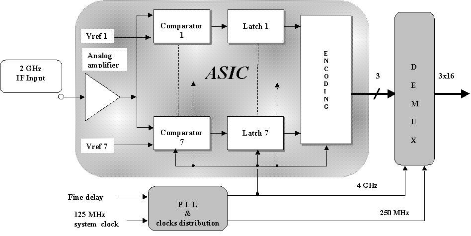
9.2.2 Digitizer Overview
The block diagram of the ALMA digitizer is given in Figure 9.2.1. It includes several fundamental elements briefly described in the following Section. The input adapter amplifier, the comparators and associated latches and encoding are implemented in a single ASIC. The fast demultiplexing unit is separated from the ASIC to diminish any coupling of the digital output with the analog signal input. The ASIC and the demultiplexing unit form the digitizer proper.
The PLL box produces and distributes the sinusoidal 4 GHz sampling clock signal and the 250 MHz signal required by the demultiplexing unit. This is another separate unit which will be common to at least one digitizer pair. Fine delay setting may be obtained by controlling the sample phase in the PLL box. (Responsibility of the design of the PLL 4GHz box has not yet been attributed and is being discussed between both IRAM and NRAO.)
Figure 9.2.1 Digitizer Block Diagram
9.2.3 The Digitizers
Input Adapter Amplifier
The input analog signal is delivered from one of the four outputs (50 ohms impedance) of the IF down-converter module in the range 2 to 4 GHz. It is random with Gaussian statistics. The response of this amplifier is flat within +/- 0.5 dB over 2 GHz bandwidth and linear up to about +15 dB above the r.m.s. input signal voltage. The voltage supply required for the adopted ASIC technology is +/-1.25 V.
The digitizer input level is controlled in the IF downconverter with +/- 0.25 dB attenuators placed in the 2-4 GHz output paths of each IF downconverter. This allows us to minimize platforming effects and to keep the quantization thresholds constant and at their optimum level for maximum quantizing efficiency.
If the dynamical tests of the digitizer prototype would not be good enough (see Digitizer Test Bench below) further downconversion to the 0-2 GHz band just before the input amplifier stage could become necessary. This would be made with 4 GHz mixing from the PLL box.
Comparators and Quantization Thresholds
The sampling function is performed in the comparators which include two latches operated in a master-slave configuration and clocked at 4 GHz. The 4 GHz clock signal is equally distributed to 7 comparators. It is shaped internally in a dedicated amplifier driven by the external 4 GHz sinusoidal signal. The seven thresholds comprise a zero reference voltage and are set around +/- 0.5 'sig' , 1 'sig' and 1.5 'sig' where 'sig' is the r.m.s. voltage at the common input of the 7 comparators; these levels are kept constant and their exact value is tuned with an accurate division voltage chain so as to minimize the quantization losses. First simulations of SiGe digitizers indicate that the sampler indecision region is small and at the level of 1% of the smallest comparison threshold.
Encoding
The digitizer encoding is not yet finally adopted. It is not dictated by the correlator specifications because the digital FIR filters have look-up tables to translate between the digitizer code and the 4-level correlator chip code. However, the encoding should minimize the power consumption and should permit easy identification of the digitized signal sign (Walsh demodulation). We plan to deliver SCFL differential logic levels.
Adopted Technology
At the moment, the adopted technology is based on high speed SiGe bipolar transistors from ST-Microelectronics. In order to check the technology performances, the layout of an experimental ASIC comprising an input amplifier, two comparator-latches, two output buffers and clock distribution has been prepared with design tools and verification software from ST-Microelectronics. Simulations are encouraging and a first layout has been sent to the foundry. The technology will evolve from BiCMOS6G to BiCMOS7G all designs being made with 2.5 V DC supply voltage.
Packaging
The encapsuled sampler ASIC (as delivered from the industry) will be placed on a printed board and in a shielded enclosure with coaxial connectors. Each three bit output is sent through a coaxial connector to the input of each single bit demultiplexing board (if option a) described below in the Interface to the Data Transmission System is adopted), and each board is placed in a separate shielded enclosure. Shielding and coaxial connectors will minimize cross-talks and digital feedback to the sampler input.
Digitizer Test Bench
Thorough tests of the digitizer ASIC prototypes will be undertaken on a dedicated test bench. This bench comprises a broad band input noise source with low / bandpass filters (0-2, 2-4, 0-4 GHz). The 3-bit output data from the sampler ASIC are sent to a Fast Demultiplexing Unit (FDU) with 2 logic layers and synchronizers. The FDU data are then processed in a simplified (16 lags) low frequency correlator based on FPGAs. The demultiplexing stage of the test bench is identified as a 'risky' area in the design. Figure 9.2.2 shows the basic principles of the FDU.
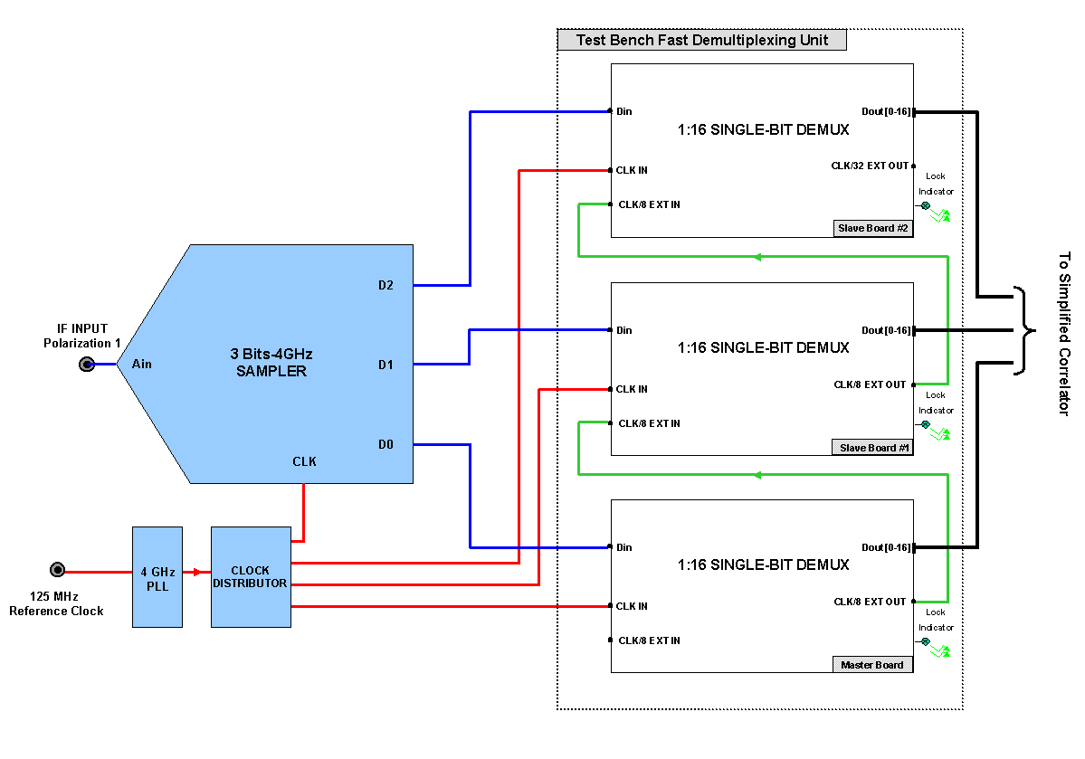
Figure 9.2.2 Test Bench Fast Demultiplexing Unit (FDU) Block Diagram
The FDU is made up of three single bit demultiplexing boards. Each board comprises a 1:16 demultiplexer and a synchronizer allowing multi-bit demultiplexing operation. The 1:16 demultiplexer consists of several logic layers the first one using commercial high speed GaAs ICs. The synchronizer can be seen as a PLL stage detecting whether the (equivalent) 1:16 logic counters of two chained demultiplexers operate in the same phase state or not.
Interface to the Fiber Optic Data Transmission System
Designing a series-reproducible version of the test bench FDU poses a significant problem because there are no commercial demultiplexers phasing 3 bit signals at high rates. We envisage three main possibilities: a) synchronize the three single bit commercial demultiplexers as performed in the test bench; b) use commercial high speed gate arrays, if available; c) develop a new ASIC. While option b) needs to be investigated carefully, we do not know at the moment whether it will be reliably possible with option a) to go to the production stage for hundreds of units.
The demultiplexed output is interfaced to the Virtual Parallel Bus (VPB) transmitter. It delivers 16 times 3 bits or 48 lines at 250 Mbps consistent with the 12 Gbps output data flow from each sampler ASIC, and consistent with the input of the VPB digital serializer and optical combiner needed for the IF/FO downlink.
We propose to place a digitizer pair (twice 2 GHz IF from two polarizations) and their 6 associated demultiplexing boards (option a) above) within another bigger shield to deliver 96 lines to the digital block of the VPB transmitter. Common shielding with the digital and optical VPB blocks should also be investigated provided that there is no RFI damage.
Alain Baudry
revised, 19 January 2001
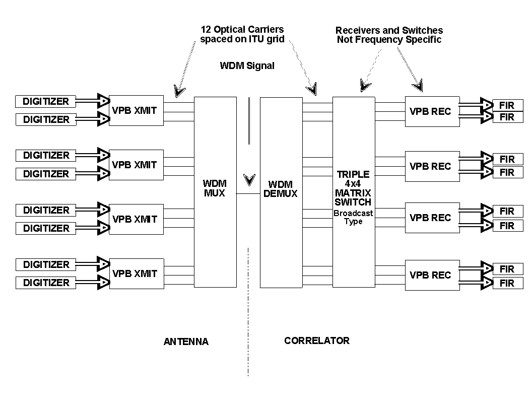
9.3 The Digital Fiber Optic Data Transmission System
The current hardware design of a Virtual Parallel Bus (VPB) system for the serialization, synchronization and transmission of the digital IF data from the ALMA interferometer antennas to the correlator is presented here. The transmission protocol will be presented in a future ALMA memo entitled "Digital Transmission System Signaling Protocol" by Robert W. Freund. The fiber optic IF link for the Atacama Large Millimeter Array (ALMA) and the ALMA Test interferometer utilize the same design.
The Virtual Parallel Bus system accepts 96 bits of parallel 250 Mbps data from a pair of digitizers in the antenna and transmits it over a fiber optic cable to the Correlator. The system includes a digital multiplexer, an optical transmitter composed of a laser and electro-absorptive modulator, a wavelength division multiplexer, single-mode fiber, optical de-multiplexer, an optical receiver, and finally a digital de-multiplexer.
Twelve links will be needed for each antenna in the ALMA array in order to transmit 3-bit data from eight digitizers to the Central Electronics Building. A full twelve-carrier system is shown in Figure 9.3.1.
Figure 9.3.1 Intermediate Frequency Fiber Optic System Block Diagram
9.3.1 Transmitter
A block diagram of a single IF data transmission channel for the Digital Fiber Optic IF Transmitter is shown in Figure 9.3.2. The current design contains all of the multiplexing and electrical to optical conversion on a doublewide AT style module with connections to the digitizers via a backplane board or high-density cable(s). The optical to electrical conversion hardware includes the laser with an integrated Electro-absorption modulator, and laser temperature and bias current control hardware. In addition, there is a provision for an optical wavelength locker and the associated feedback control circuit. Optical power monitoring is handled through the interface to the Laser Driver module. The card is controlled by a Monitor and Control (M&C) interface.
The following list specifies the components in transmitter module.
Power Supply: The board contains on-board regulators to produce the various voltages required by the VPB from the 48-Volt DC input voltage. The voltage requirements are +1.8VDC, +2.5VDC, +3.3VDC, +5.0VDC, -5.2VDC, and +8.0VDC. Other voltages may be required and can be produced with inexpensive 48VDC input switching regulators.
On-Board Control System: The on-board control for a single VPB transmit module consists of three devices, an AMBSI2 (formerly known as ZASI) module and two PIC 16C74 microcontrollers. The first 16C74 microcontroller controls internal operation of the three XILINX Virtex–E FPGA’s. The second PIC 16C74 microcontroller provides all necessary monitor and control functions required by the three laser power controllers and the three laser temperature control modules. Both 16C74 microcontrollers communicate with the AMBSI2 via an SPI bus connection. The AMBSI2 module interfaces to the CAN based ALMA Monitor and Control System.
Clock distribution: This block uses the 125 MHz sine-wave system clock for the generation of a 625 MHz clock for the 10Gbps Multiplexer IC, and a 312.5 MHz clock for the FPGA. The board also requires a 20.833 Hz signal at LVDS levels,
625 Mbps Serializer/Protocol Engine: A Xilinx Virtex-E FPGA. This device will contain all of the logic for multiplexing the 250 MHz input data up to the 625 MHz rate required by the 10Gbps Multiplexer IC. It also provides all framing and synchronization functions as described in the Signaling Protocol document.
10 Gbps Serializer: This consists of a Giga GD16555/85 10Gbps multiplexer IC and associated electronics. The multiplexer converts the 625 MHz 16-bit parallel data into a 10 Gbps serial data stream for transmission over the fiber optic link. This circuit is essentially as shown in the data sheets, application notes and evaluation board design from Giga.
Driver Amplifier: Amplifies differential CML output of 10Gbps Multiplexer IC to sufficient levels to drive the optical Electro-Absorption Modulator (EAM).
Optical/RF Board: This includes the integrated laser / EAM package plus the laser power and temperature controllers.
Wavelength Locker: This is an optional item and is not shown because it is not necessary for the basic operation of the system. It may be necessary to use a wavelength locker and feedback control to keep the operational frequency of the laser from drifting out of the passband of the DWDM components and to minimize time-of-flight variations due to frequency dependence of the index of refraction in the fiber. It is estimated that lasers currently available may drift out of the optical passband of the DWDM components in 2 to 4 years time. However, new components are becoming available in the market that advertise ultra-stable frequency operation, maintaining operation in a 100 GHz bandwidth over as much as 20 years, which would obviate the need for wavelength lockers. Wavelength lockers are not an attractive option because of their extremely high cost. Wavelength lockers currently cost over $1,000 each and require additional circuit complexity to implement.
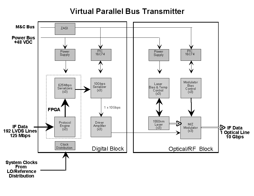
Figure 9.3.2 Transmitter Block Diagram
Packaging
: The Transmitter will be mounted in a doublewide RFI shielded Australia Telescope (AT) style module. Data will be fed into the modules on high-density connectors through a backplane or high density shielded cables. The choice of connection method will be driven primarily by RFI considerations The transmitters will have a minimum of two printed circuit boards, one carrying the digital electronics and M&C interface, and the other holding the Optical components and associated electronics. The separate Optical board simplifies sparing since each laser must be tuned to an operational frequency in order to match the transmission passbands of the DWDM components while the digital boards are consistent throughout all VPB modules. Figure 9.3.3 shows a conceptual drawing of the VPB transmitter module. A third mezzanine board may be used for the 10Gbps multiplexer IC to simplify replacement of that device due to a rapidly changing market.
The output of this transmitter module is three optical carriers that will be combined with the carriers from the remaining three VPB modules using WDM techniques for transmission to the VPB receivers in the correlator rack over a single fiber. Connections to the optical fibers from each module are made through Diamond E-2000 blind-mate backplane connectors. The use of blind-mate backplane connectors reduces maintenance costs by enabling easy replacement of the modules, and significantly reduces the chances for damage during replacement. The fibers are all routed to a separate DWDM module
.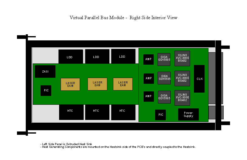
Figure 9.3.3 Conceptual diagram of a two channel Transmitter Module.
9.3.2 Receiver:
Figure 9.3.4 shows the functional block diagram of a receiver. The optical signal is received by a pin photodiode and the photo-generated current is used to recreate the 10Gbps digital signal, and to determine the average received optical power. The relatively weak digital signal is passed on to an amplifier that generates the voltage levels needed by the demultiplexer, which converts the data into 16 parallel streams at 625 Mbps. The FPGA does the final demultiplexing to 64 streams at 125 Mbps.
PD & Amps: This includes a pin photodiode, amplification stage, and an optional electrical filter. The output is a 10 Gbps data stream that is fed to the 10 Gbps Demultiplexer IC. The electrical filter is a low cost item that is typically used for SONET applications in the telecom industry.
10 Gbps demultiplexer : The first demultiplexer stage is a Giga GD16544 or GD16584 10Gbps demultiplexer IC and the associated electronics. It converts the 10 Gbps serial data stream from the fiber optic link to 625 MHz 16-bit parallel data. This circuit is essentially the same as shown in the data sheets, application notes and evaluation board design provided by Giga.
Receive Shift Register/Protocol Engine: A Xilinx Virtex-E FPGA converts the 16 bit 625 MHz data from the demultiplexer IC into 80 bit 125 MHz data for presentation to the Correlator. The FPGA implements all synchronization, timing and data integrity functions as described in the Signaling Protocol Document.
On-Board Control System: The On-board control for a single VPB receive module consists of three devices, a AMBSI2 module and two PIC 16C74 microcontrollers. The first 16C74 microcontroller controls internal operation of the three XILINX Virtex–E FPGA’s. The second PIC 16C74 microcontroller provides all necessary monitor and control functions required by the three optical receivers. Both 16C74 microcontrollers communicate with the AMBSI2 via an SPI bus connection. The AMBSI2 module interfaces to the CAN based ALMA Monitor and Control System. A list of interface commands has been generated, but needs revision to reflect the M&C protocol. Further modification to this list will also be necessary as the design evolves. This information will be detailed in the appropriate Interface Control Document.
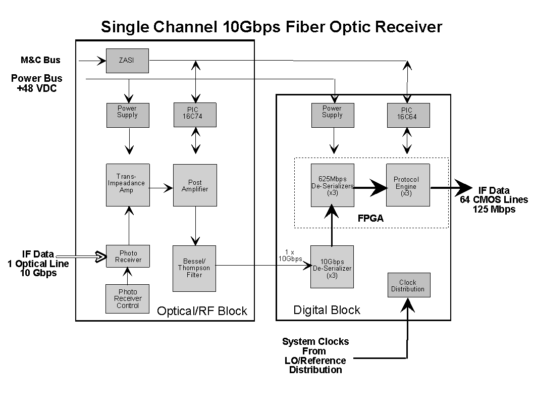
Figure 9.3.4 Receiver Block Diagram
Packaging
: The VPB Receiver is packaged in a 6U x 280mm size Euro Card of the same general design as the cards in the ALMA Correlator. These boards will be installed in the correlator rack with the FIR filter cards. The optical portion of the module is on a separate card to aid in sparing and future modification issues. Heat generating components are cooled with individual heatsinks bonded to the components. Figure 9.3.5 shows the VPB Main Boar d and Figure 9.3.6 shows the Optical Board.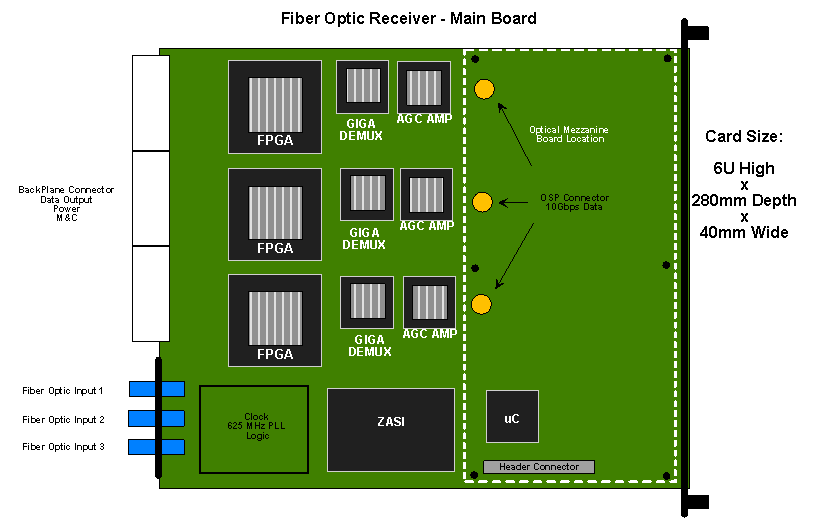
Figure 9.3.5 VPB Receiver Main Printed Circuit Board
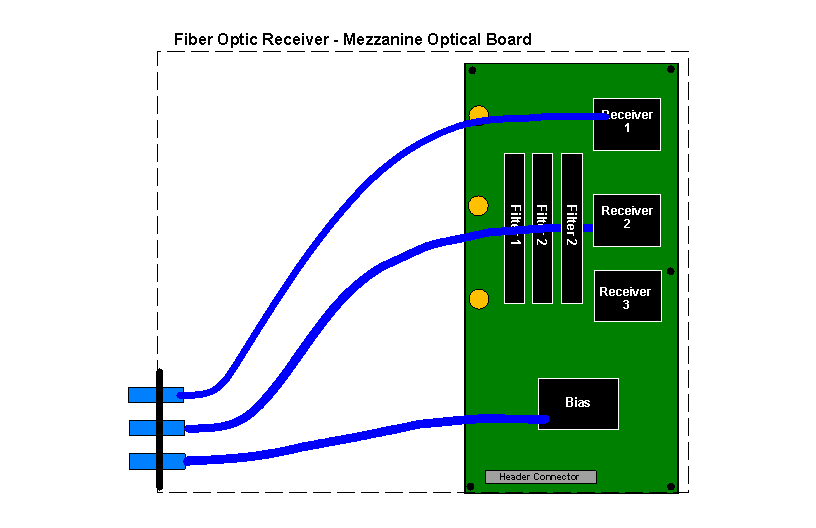
Figure 9.3.6 VPB Receiver Optical Mezzanine Board
Jim Jackson
2001 January 22
Figure 9.1.1 Block Diagram of Downconverter