Fig. 1
MMA Project Book, Chapter 7 Section 1
John Payne
Bill Shillue
Andrea Vaccari
Last changed 01 July 1999
Revision History:
1998-07-27: First version
1998-11-13: Major revision
1999-04-13: Major revision (Phase
noise analysis of the locked lasers, Review of commercially
available detectors, Photomixer develpment)
1999-07-01: Text formatting problem
fixed
Summary
Recent commercial developments in the optical fiber industry have raised the possibility of supplying the local oscillator signal for the MMA by generating two optical signals differing in frequency by the required local oscillator frequency. These two optical signals may then be transmitted over a single optical fiber to each antenna. Within the receiver dewar, the two optical signals are mixed in a photodetector and the resultant millimeter-wave frequency difference supplies the local oscillator power.
Table 7.1 Principal milestones for photonic local oscillator.
Task |
Completion Date |
|
1) |
Demonstration of adequate spectral purity between phase-locked lasers. |
Done 8-98 |
2) |
Test and evaluation of 100 GHz photodetector |
05-99 |
3) |
Measurement of single MSM photodiode |
05-99 |
4) |
Design matching network for single photodiode |
07-99 |
7.1 Introduction
The local oscillator system for the MMA presents a great challenge for the instrument builders. The generation of a pure frequency with high phase stability in the frequency range of 90-900 GHz at each of forty antennas, and preserving the phase relati onship between antennas for long (perhaps hours) periods of time, is perhaps the most difficult part of the instrument. Although, in theory, the task could be completed with components available today by adopting the conventional route of a phase-locked o scillator at a frequency of around 100 GHz, followed by multipliers, the cost and complexity are daunting. There have been recent developments in the so called "conventional" techniques that suggest that the reliability and cost of this approach may be gr eatly improved by the application of new beam lead diodes and MMICs, and we are pursuing this approach as described in Section 2 of this Chapter.
However, recent advances in laser diode technology and optical fiber transmission systems raise the possibility of a local oscillator system for the MMA, based on the mixing of two optical signals separated by the required local oscillator frequency. S uch a system could be realized using mainly commercially available components, resulting in significant savings in both cost and manpower when compared to the conventional approach of a phase locked oscillator followed by passive multipliers. This approac h is so attractive that we have mounted a development effort to investigate the feasibility of such an approach.
Several groups have worked on systems similar to this. The phase-locking of the beat note between two infrared lasers to an external microwave standard, with the spectral purity required of the MMA, was first demonstrated many years ago and is now rega rded as routine. (For references and more details, see MMA memo #200). Beat notes of up to several THz have been demonstrated with a cooled fiber-coupled photomixer at power levels that appear to be marginally adequate for supplying the LO to the SIS rece ivers on the MMA. New detector fabrication techniques hold the promise of increased power levels in the wavelength range of the MMA.
The potential advantages of such a system may be summarized as follows:
The majority of the components needed for the realization of the proposed scheme are commercially available. The communications industry has a huge investment in optical fiber systems, and the system outlined here exploits these fairly recent developme nts. We can be certain that intense development in this area will continue.
All of the frequency synthesis components of the local oscillator system may be situated in a laboratory environment remote from the array. At the antennas, only some leveling electronics and a photomixer are required. In terms of serviceability an d reliability, this is regarded as a great advantage.
The receiver interface is greatly simplified. Due to bandwidth requirements, the usual Martin-Puplett quasi-optical LO injection scheme will not be appropriate. LO injection using conventional methods with waveguides entering into the cryogenic enc losure (for each receiver band) would involve a relatively high loss and would complicate the thermal design of the receiver. In contrast, all that will be needed in the photonic system is one optical fiber into the receiver dewar resulting in negligible heat load. Vacuum feed-throughs for fiber are fully developed commercially.
There is a great reduction in complexity .
The proposed system eliminates the need for the usual microwave harmonic mixers.
The real cost promises to be far less than a conventional system.
In the conventional system the passive multipliers following the fundamental oscillator introduce additional amplitude and phase noise. Investigation is needed here but it seems possible that noise on the fundamental oscillator may be multiplied by the square of the multiplication ratio. In the case of multiplying from 100 GHz to 800 GHz, phase noise enhancement by factor of 64 may well be involved which could prove unacceptable for use in the array. It may be that such an effect is absent in the c ase of the photonic system although work is needed to settle this question.
Details on the following are given in MMA Memo 200 , Photonic Local Oscillator for the MMA.
MMA LO requirements.
Description of proposed system.
Theory of photo-mixing.
Expected performance.
References.
7.2.1 Tests on prototyper system
We have conducted several experiments concerninc the phase locking of the beat frequency between two 1.5 micron lasers to a microwave standard. So far our experiments have been confined to frequencies obtainable with commercially available detectors, t hat is 60 GHz. The questions that we have attempted to answer in the first round of experimnts are the following:
Is the phase locked difference frequency "pure" enough for the MMA application?
Are the characteristic of the difference frequency independent of the value of the difference frequency? Due to the fact that the difference frequency (up to 1 THz) is derived from lasers oscillating at 200 THz it would seem that any sources of noise would not change in value for changes in difference frequency. Using commercially available components up to 50 GHz it should be possible to prove this.
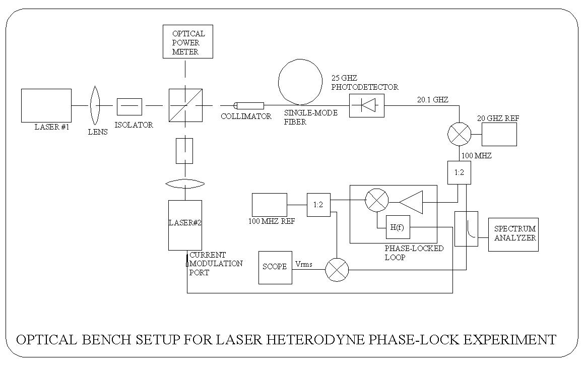
A block diagram of the experimental set-up is shown in Fig. 1.
Fig. 1
We have used both external-cavity diode lasers and an erbium-doped fiber ring laser. This latter type of laser is known to have exceptional frequency stability and a linewidth on the order of 5 kHz. In Fig. 1, the output of the fiber laser with wavelength of 1.55 microns is combined with the output of an external cavity diode laser and the resultant beam is directed to a high frequency photodetector. Conventional phase locking circuitry is then used to lock the difference frequency to a fre quency standard which may be tuned from around 200 MHz to 20 GHz. As may be seen from the block diagram the intermediate frequency in the phase lock system is 100 MHz. The spectrum analyzer can be used to monitor the 100 MHz phase-lock IF as in the figure, or the actual beat-note frequency if a directional coupler is inserted between the photodetector and the mixer. This system had remained locked for over one week of continuous use.
A typical result from the phase lock system is shown in Fig. 2.

Fig. 2
The spectrum of the lock signal is clean, with the linewidth measurement being limited by the resolution bandwidth of the spectrum analyzer. The phase-locking has been done at many different lock frequencies, to determine if the noise prope rties of the beat-note are affected by the lock frequency. In Fig. 3, the phase-lock spectrum is shown over a 100 kHz span at lock frequencies of 1.1 GHz, 5.1 GHz, 10.1 GHz, 15.1 GHz, and 20.1 GHz. The reference level for each spectrum is offs et by 10dB from the previous one. Clearly, there is no noticeable frequency dependent difference. (Note: The 20.1 GHz spectrum looks different because the offset that was introduced caused the spectrum to go below the analyzer's noise floor).

Fig. 3
A more accurate measurement of the phase spectrum of the beat-note is provided by a phase measurement utility written by HP for their HP8563E analyzer. The routine acquires spectra at multiple spans and bandwidths until a complete plot of the pha se noise versus offset frequency is compiled. This plot is shown in Fig. 4 for a 20.1 GHz beat-note. Note that the loop bandwidth of 200kHz is clearly evident. Outside this bandwidth the phase is that of the combination of the two free-r unning lasers. Within the loop bandwidth, the noise is as low as -88 dBc/Hz. Below 10 kHz, there are some phase noise contributions believed to be from the manufacturers laser controller and not inherent to either of the two lasers. This we expect to improve upon. Also, if one integrates the noise across the spectrum to get the total phase error, we are currently achieving about 0.17 radians. Although this is within the toerance of phase error for the MMA, it is our hope to i mprove the total phase error from this value. The major contributions to phase noise are coming from 50 kHz offset to 1MHZ offset, so if we increase the loop bandwidth then we expect a phase noise reduction. As an additional note, the phase no ise plot shown in Fig. 4 was repeated for several different lock frequencies, with the same result anywhere in the 1-20 GHz range. We are therefore confident that there are no hidden factors that would cause the phase noise to be any worse at 100 GH z or 1 THz, especially if the promising techniques of optical phase-locking are shown to work.

Fig. 4
7.2.2 The photodetector. Commercial devices.
At the heart of the laser LO scheme is the photodetector. The following is a summary of the state of the art in commercial devices.
7.2.2.1 High-Speed Photomixers for Radio Astronomy
This memo summarizes the state of research in high-speed photodetectors (also referred to as photomixers) in the 100 GHz-2 THz range, and discusses some of the technical factors which are affecting the development of these devices.
7.2.2.2 Device Basics
Photodetectors generally consist of a semiconductor material which has a bandgap energy such that it is sensitive to light in a certain wavelength range; and a photon of light can cause the generation of an electron-hole pair which under an applied ele ctric field causes a current to flow.
The photocurrent generated in a photodetector is given by [1]:
The amount of RF power generated in a heterodyne application goes as the square of the device current. Therefore, desirable parameters are high quantum efficiency, h, high optical power, Popt, longer optical wavelengths, 1/n, longer carrier recombination lifetimes,t , fast carrier drift velocity, Vd, and s hort device lengths, l. There follows a discussion of some of these parameters as it pertains to generating a terahertz photomixer for radio astronomy.
7.2.2.3 High-Speed Device Limitations
Two important parameters that governs response speed are the carrier recombination time, t, and the carrier transit-time l/Vd (device length divided by drift velocity). Vd is determined by the material, the field created by the junction, and by any reverse bias of the junction. If the field is high enough, the carrier velocity saturates. Carriers must have a short transit-time in order for the device re sponse speed to be high, because this is the time required for carriers that are generated furthest away from the terminals to drift to the terminals under the influence of the electric field in the active area. Clearly, for short transit times the device length must be kept small.
Having established that small device lengths would seem to be required for high-speed photomixers, two deleterious effects of short device lengths arise. First, a small device length means a small active area so there is less light gathering cross sect ion and the proximity of the terminals to each other raises the device capacitance. This leads to an RC-time-constant that limits the output frequency response to f=1/tRC. Clearly then, there is a limit to how short the device length can be made because at some point increasing device capacitance slows the response and negates any gains made by shorter transit-time. The second undesirable effect of a short device is that the cross-sectional area of the device is decreased and thus fewer photons are detected, lowering the device current and output power.
7.2.2.4 Traveling-Wave and Velocity-Matched Photodetectors
To overcome these difficulties, the leading researchers in high speed photodetectors have been investigating traveling-wave or velocity-matched devices.[1, 2] These techniques are being actively pursued at UCLA, UCSB, JPL-Caltech, and several r esearch institutions in Europe. In the traveling-wave detector, the active area is elongated in one dimension and the output current is collected in a traveling-wave structure such as coplanar waveguide. In the velocity-matched device, the output power fr om many high-speed photodetectors is combined coherently.
In the velocity-matched photodetector, the device speed is limited by the response speed of the individual photodetectors and by the degree to which the velocities are matched. The optical wave from the laser light must travel at the same speed as the RF-wave in the output structure. Researchers have shown that this gives an upper limit to the device speed because of the dispersion of the output structure, such as coplanar waveguide. However, this applies only to a device that must work from DC to some upper bandwidth limit, such as a 500 GHz oscilloscope pulse detector. For heterodyne applications such as envisioned for local oscillators for radio astronomy, the output bandwidth of the device could be limited to say, 200-300 GHz, in which case it is o nly necessary to match the wave velocities from 200-300 GHz while taking the dispersion into account.
Recently, two research groups have developed techniques for achieving a velocity-matched photodetector with the optical coupling to the device in free space.[1, 2] The benefit is that a complicated optical waveguide coupling structure is not re quired, just a fiber and a lens. Also, the velocity-matching is tuneable by changing the angle of the light that is incident on the photodetector.
Another technique has been used to achieve very high-speed response. If the carrier recombination time is long compared to the transit-time, then the device is said to be transit-time limited and the physics discussion above applies in full. However, i f the recombination time is shorter than the transit-time, then some carriers are recombining before they have reached the device terminals and they do not contribute to photocurrent. The transit-time can then be made significantly longer than the recombi nation time, and the device will still have a high speed operation because only the carriers excited near the device terminals are contributing to the photocurrent. The main drawback is that the device responsivity goes down significantly due to the recom bination, and the device current and output power are decreased. Devices have been built using this principle for 800 nm operation using low-temperature grown GaAs, which has carrier lifetimes as short as 90 fsec.[6, 7] Unfortunately, the bandgap of Lt-GaAs is more suitable for operation at 800 nm than 1550 nm, and little work has been done on 1550 nm materials with short lifetimes. However, recently, some work has been done in that area with encouraging results.[8] In this work, the InGa As material was implanted with impurity ions to reduce the carrier lifetime, and a noticeable increase in device speed was achieved. The same group has done work on wideband distributed photodetectors, and it would seem that a high-speed traveling-wave ph otodetector in ion-implanted InGaAs would be a logical extension to their research.[9]
7.2.2.5 Cooling of the devices
Cooling of high-speed photodiodes has the potential for several interesting and beneficial effects. One research team has developed photodiodes that have a bandwidth of greater than 1 THz, and an output power of 0.2 mWat 800 nm.[5] Because of the short carrier lifetime, the devices are very inefficient and the power limit is due to self-heating rather than saturation. It is quite possible that thermal failure limits of this sort can be alleviated by cooling the device. A second beneficial effect of cooling is that the device should have a wider bandwidth. At lower temperatures, carrier mobilities increase and even carrier saturation velocity increases in III-V materials, so the device speed should increase if the dev ice is transit-time limited. If the device is RC-constant limited then the speed will also increase due to the lower resistivity of most metals at lower temperature. The improvements in device performance at low temperature are not expected to be order of magnitude, but more like 20-30%, although this is only an educated guess and device testing will have to be the final arbiter. Another effect of cooling will be to change the spectral response. Due to the change in the bandgap energy with temperature, th e spectral response curve will shift to shorter wavelengths at about 0.5-1.0 nm/deg C.
7.2.2.6 Device Output Coupling
For AC photodetection such as demodulation or optical heterodyning, the photodetector must have an appropriate radio frequency (RF) circuit to collect the photo-generated carriers. For heterodyne applications above 200 GHz, the output power must be cou pled into a fundamental waveguide mode or via some quasi-optical means. For radio astronomy applications, the output will be used to drive an SIS mixer, and careful design of the means of coupling this power to the SIS mixer is necessary. Preliminary work in this area has consisted of arranging a velocity-matched photodetector on an InP substrate, with an output coplanar-stripline (CPS) that has an integrated Yagi-antenna probe that radiates into fundamental WR-10 waveguide across the 75-110 GHz band.
Besides matching into fundamental mode waveguide, there is also the issue of the match between the load impedance and the device impedance. Generally, high frequency photodiodes look like a current source with a small parallel capacitance. However, the re may be leakage resistance, contact resistance, and input inductance as well. In general, the impedance can be matched quite well to an arbitrary load but only over a limited bandwidth. Because the majority of applications for high-speed diodes has been in short-pulse generation and communications, there has been little interest in device matching because it would limit the bandwidth. For heterodyne generation of millimeter-wave local oscillators, however, bandwidths comparable to millimeter-wave receiv er bandwidths, in the 25-40% range, are acceptable.
7.2.2.7 Commercial Detectors
More photodetectors are being developed for the DC-50 GHz range every year, and several have been developed just in the past year that have significantly higher output current than was previously available. In fact, with 5-10 mA of current, these devic es potentially have enough power to drive an SIS receiver with a single photodiode device, especially if matching of the device output impedance were done. None have even been tested above 50 GHz, but if the degradation above 50 GHz is graceful, then it i s not inconceivable that they could be used for the 68-120 GHz frequency range. The table below shows the best performance that is currently available in 1.55 micron photodetector.
Vendor |
Part Number |
3dB Bandwidth |
Responsivity mA/mW |
Current |
Price |
NTT10 |
KEPD2525VPG |
50 GHz |
0.9 |
6.3 mA |
$10,700 |
NTT |
KEPD2535VPG |
50 GHz |
0.9 |
11.7 mA |
$11,290 |
Discovery11 |
DSC10S-3 |
50 GHz |
0.5 |
5.0 mA |
$6500 |
OptoSpeed12 |
PDMH40B |
45 GHz |
0.5 |
5.0 mA |
$6100 |
Table 1: High Speed Photodetectors, Manufacturers, and Specifications
7.2.2.8 Development Course
As with many development projects the time scales are uncertain but the following (Table 7.2) is an estimate of the times for the various tasks that have to be completed to bring the development project to completion.
Table 7.2
Task |
People |
Completion Date |
|
1) |
Set up two external cavity lasers phase locked to a microwave ref. Measure phase and amplitude noise at beat frequencies up to 18 GHz. |
1 EE |
8-98 |
2) |
Design and build the optical comb generator. |
1 EE + 1/2 Tech |
7-99 |
3) |
Test comb generator up to 80 GHz using commercial detectors. |
1 EE + 1/2 Tech |
7-99 |
4) |
Test and evaluate 100 GHz UCLA photodetector |
1 EE + 1/2 Tech |
6-99 |
5) |
Test and evaluate UCLA photodetector at 230 GHz |
1 EE + 1/2 Tech |
12-99 |
6) |
Complete laboratory test using two 230 GHz photodetectors. |
1 EE + 1/2 Tech |
5-00 |
7.3 Summary of photomixer development
7.3.1 Choice of 1.55 micron optical wavelength
It was decided in June of 1997 that NRAO should pursue the development of high speed photomixers as a competitive technology for the generation of local oscillator signals in SIS receivers for the Millimeter Array. Although some work had been don e on photomixers with response at up to a terahertz, those photodiodes provided very low power levels, and were very inefficient. For this reason, a velocity-matched photodetector seemed like the best approach. Of the few research groups that were known to be capable of developing this type of device, UCLA was the most eager to collaborate with NRAO. Their previous work had been done at 800 nm optical wavelength, and device speeds of up to 50 GHz were achieved. The overall ph otonic LO concept required a low-loss long-distance distribution of the photonic signals to each antenna, and thus the use of wavelengths either in the 1300 nm or 1550 nm optical wavelength window would be required. Therefore, a contract was agreed to between NRAO and UCLA whereby UCLA would endeavor to develop new VMDP devices that would work at 1550 nm, and that would work over the 75-110 GHz waveguide bandwidth. The development effort was two-fold: first UCLA had to convert their photolitho graphy and device fabrication to work with InGaAs and InP materials rather than GaAs, and second, the target output bandwidth of the devices would go to significantly higher frequency. Although 110 GHz is still well below the frequency range that wi ll ultimately be required for the MMA, it was felt at the time that an incremental development approach would be the wisest course. It should be remarked upon, however, that in the literature and in the jargon of those who work on these ultrafast ph otodetectors, device bandwidth is taken to mean the 3dB bandwidth. However, since a given MMA receiver will use only one frequency at a time, the bandwidth of the photdetector is not really important. The power out of the device at the given f requency is what matters, and it will very likely be possible to get sufficient power out of a device at frequencies well above the 3dB bandwidth.
7.3.2 100 GHz VMDP photomixer description
The basic operating principle of the velocity-matched photodetector (VMDP) is well described in [[2] Ming Wu et al, "Velocity-Matched Distributed Photodetectors with High-Saturation Power and Large Bandwidth", IEEE Photonics Technology Letters, Vol. 8, No. 10, Oct 1996, pp.1376-8]. Shown in Figure 5 below is a schematic of a typical VMDP. The light is input at one end from an optical fiber and then travels down the length of the wafer inside of a semiconductor optical waveguide. The w aveguide is designed in such a way that some of the light travel near the surface of the wafer and is coupled to each of several photodiodes which are periodically spaced on the surface. The photodiodes each have two terminals, a cathode and an anod e that are formed by very tightly spaced interdigital metal fingers on the surface of the diode. These fingers are then connected to the coplanar striplines that form the RF transmission line. The output RF traveling wave is excited at o n end, starting with the first diode, and travels along the transmission line with power from each photodiode adding coherently to the output wave. The velocity of the optical wave traveling inside the InAlGaAs ubstrate is slower than a typical micr owave transmission line structure, but the addition of the photodiodes to the transmission line has the effect of adding a distributed capacitance that slows down the microwave structure. With the right periodicity and size of photodiode the two velocities can be made to match.
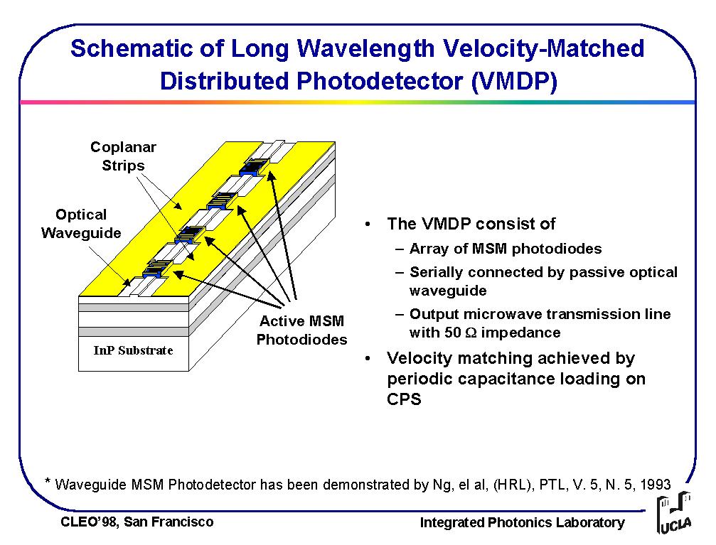
Fig. 5
7.3.3 Photomixer Output Transition to Waveguide
The design of a transition between coplanar-stripline (CPS) and fundamental mode waveguide was pursued as a separate task by the UCLA microwave group (whereas the photomixer development was done by the photonics group). It became clear after the first year of their work that the transition posed some serious challenges. First, the design of an efficient mechanism for launching a wave off of a substrate that has a high dielectric constant (InP dielectric constant =12) generally includes a lo ng antenna structure, especially if it must work over an appreciable bandwidth. The UCLA group was opposed to a long structure because it would use up a lot of space on the wafer, and spent a lot of effort in keeping the transition length short. The other difficulty in working with a high dielectric constant substrate is that spurious modes can be excited in the substrate that can compromise the performance of the transition if they occur in the output bandwidth. Thus, considerable effort was made by parties both at NRAO and UCLA to eliminate these modes, and if they were to occur, then dimensions of the output circuit were chosen to force the modes to occur outside the band. The transition was designed using a high-performan ce electromagnetic simulator.
7.3.4 UCLA Development Summary and Status
A design and development contract was let to UCLA in July of 1997 for a 100 GHz 75-100 GHz photomixer. The first year of the contract was spent converting their fabrication process from 800 nm to 1550 nm. Also, a low frequency scale m odel photomixer was fabricated as a test of the process. The test was deemed to be successful, but there was a problem that was only realized at a later date. In September of 1998, a 100 GHz VMDP photomixer was fabricated and tested in chip form at UCLA. The device response fell off severely above 10 GHz. This was also the problem with the initial test chip, but it was not noticed because the chip was designed for a lower frequency anyway. The UCLA photonics group considered several possibilities for the poor performance and designed a test that would help in this determination. The problem turned out to be that the optical waveguide did not properly confine the input light beam to the area of the photodiode which was u nderneath the metal fingers. When light impinged on the diode outside this small "target area", the carriers that were generated as a result had a long distance to travel before reaching the device figer terminals. The test involved making a s ingle diode with smaller active area, and illuminating it from above the chip. This test resulted in performace to 50 GHz that was limited only by the measuring equipment.
Having found the cause of the device problem, the next effort was to redesign the optical waveguide to provide better confinement of the light. To do this, a deep trough is etched in the substrate on either side of the optical waveguide and fille d with a low dielectric constant material, which confines the light in the same way as the cladding of an optical fiber works.
During this period of photonics troubleshooting, the design of the CPS-to-waveguide transition was modified several times to try to provide better return loss in the 75-100 GHz band. The resulting return loss from simulations is shown in Fig. 6.
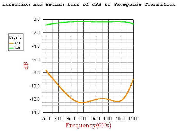
Fig. 6
Fig. 7 and 8 show a sketch of the transition. In the first figure, the VMDP chip is shown mounted at the end of the WR-10 waveguide. Only one half of the split block WR-10 waveguide is shown for clarity. The VMDP chip is soldere d to the end of a small metal block that sits in a groove in the bottom half of the split block. This mount has a small protrusion that extends slightly into the waveguide channel. In the second figure, a slightly enlarged view shows the end o f the WR-10 waveguide channel, the mount, and the VMDP chip which is comprised of photodiodes arayed across a CPS stripline and an integrated Yagi antenna. The Yagi antenna radiates into the E-plane of the waveguide. The optical fiber is input from the right hand side of the figure, with its position accurately controlled by a micropositioning stage. When the fiber-to-chip coupling is optimized, the fiber will be epoxied in place close to the chip, and also towards the end of the block to prov ide added strain relief.
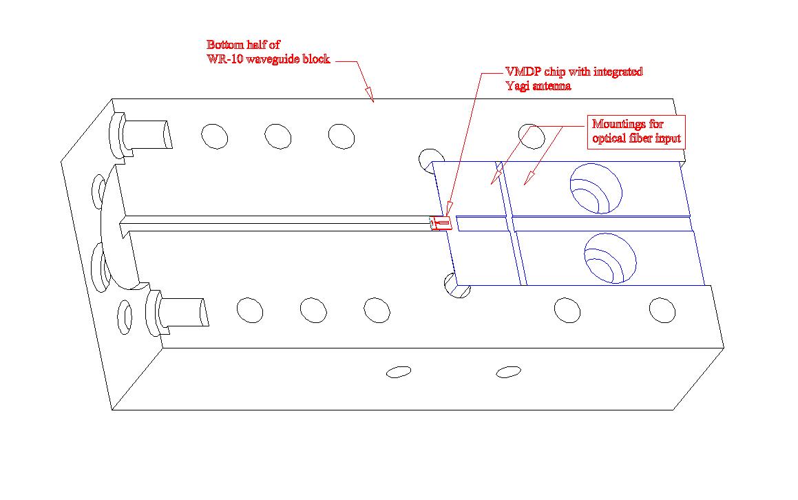
Fig. 7
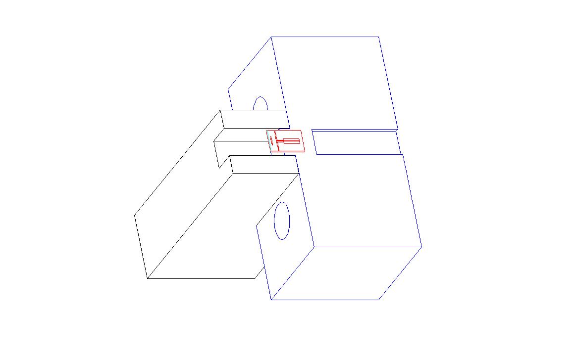
Fig. 8
7.3.5 Continuing Work
The next fabrication of a VMDP is in progress (mid-April 1999), with electron-beam lithography of the sub-micron photodiode fingers taking place at the Cornell Nanofabrication Facility. The wafer will consist of VMDPs in several different configu rations, consisting of 1,3,5, 7, and 10 photodiode VMDPs. In additon, some of the VMDPs will be fabricated with integrated transitions. It would have greatly reduced the wafer yield if all of the VMDPs had integrated transitions, because of th e wafer real estate required; and the ones without the transitions can still be tested with high frequency microwave probes. The split block photomixer housing fabrication is also in progress. The fabrication process is expected to be complete by the end of April, and the month of May will hopefully be a period of extensive testing.
7.4 References
[1] Sze, S.M., Physics of Semiconductor Devices, 1981, Wiley, Chapter 13: photodetectors.
[2] Ming Wu et al, "Velocity-Matched Distributed Photodetectors with High-Saturation Power and Large Bandwidth", IEEE Photonics Technology Letters, Vol. 8, No. 10, Oct 1996, pp.1376-8
[3] Bowers et al, "Ultrafast (370 GHz Bandwidth) p-i-n Travelling Wave Photodetector Using Low-Temperature-Grown GaAs", Appl. Phys. Letters, 71, (17), 27 Oct 1997, pp. 2508-10
[4] Matsuura, Blake et al, "A travelling-Wave THz Photomixer Based on Angle-Tuned Phase-Matching", Submitted to APL, Dec 1998
[5] Merlet et al, "A High-Speed Free-Space Travelling Wave Photodetector", Appl. Phys. Letters, 72, (10), 9 Mar 1998, pp. 1134-6
[6] McIntosh, Brown et al, "Terahertz Photomixing with Diode Laser in Low-Temperature-Grown GaAs", Appl. Phys. Letters, 67, (26), 25 Dec 1995, pp. 3844-6
[7] Vergese, McIntosh, Brown, "High Tunable Fiber-Coupled Photomixer with Coherent Terahertz Output Power", IEEE Transaction on Microwave Theory and Techniques, Vol. 45, No.8, Aug 1997, pp. 1301-1309
[8] Bottcher, Droge et al, "Ultrafast Ion-Implanted InGaAs Metal-Semiconductor-Metal Photodetectors", LEOS Symposium 1997
[9] Droge, Bottcher et al, "78 GHz Distributed InGaAs MSM Photodetector", Electronics Letters, 12 Nov 1998, Vol. 34, No. 23, pp. 2241-3
[10] NTT Electronics Corp., http://www.nel.co.jp/photo
[11] Discovery Semiconductors Inc., Princeton (NJ), http://www.chipsat.com
[12] OptoSpeed Inc., Via Cantonale, CH-6805, Mezzovico, Switzerland, +4191-946-33-34, http://www.optospeed.ch